

|
Product Details:
|
| Product Name: | 40GBASE SWDM4 | Date Rate: | 40Gb/s |
|---|---|---|---|
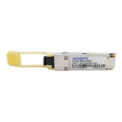
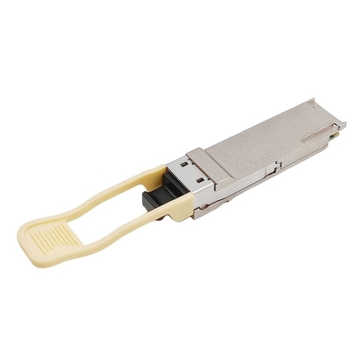
| Form Factor: | QSFP+ | Distance: | 440m@OM5/350m@OM4/240m@OM3 |
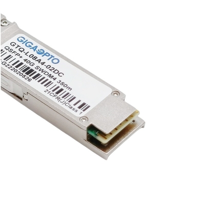
| Connector: | Duplex LC | Component: | VCSEL + PIN |
| Highlight: | QSFP-40G-CSR-S, 40G SWDM4 | ||
| Highlight: | QSFP+ MMF Optical Transceiver,850nm MMF Optical Transceiver,40GBASE SWDM4 |
||
Based on an industry multi-standard agreement (SWDM-MSA), more open interoperability than other proprietary solution like QSFP-SR-BD
Cost effectively bandwidth upgrading from 10G to 40G without changing existing fibers
Description
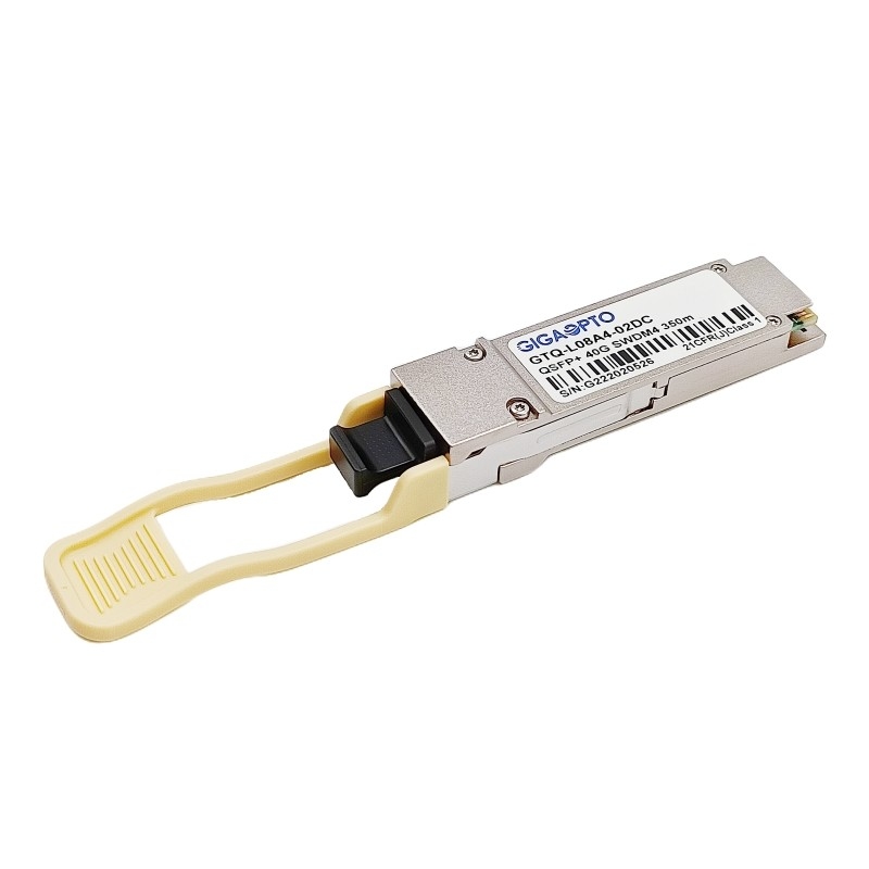
The GTQ-L08A4-02DC is a kind of pluggable optical transceiver uses SWDM (Short Wavelength Division Multiplex) technology working with multimode fiber, providing 4 channels in the 850-940nm region at 10Gbps/lanes, which can transmit a multiplexed 40G signal over wide band OM5 at lengths up to 440m(240m on OM3/350m on OM4) with an duplex LC connector.
Uses two fibers (duplex) instead of eight (SR4), this 40G SWDM4-S is a more cost effective transceiver solution for 10G to 40G migration applications.
The QSFP+ 40Gbase-SWDM4 transceivers are compliant with the QSFP+ MSA and IEEE 802.3ba XLPPI electrical interface.
Digital diagnostics functions are available via an I2C interface, as specified by the QSFP+ MSA.
Specification
| Product Category | 40Gbase SWDM4 | P/N | GTQ-L08A4-02DC |
| Form Factor | QSFP+ | Data-Rate | 41.2Gbps (4×10.3Gbps) |
| Link Distance | 440m@OM5/350m@OM4/240m@OM3 | Media Type | MMF |
| Wavelength (CH1-CH4) | 850nm, 880nm, 910nm, 940nm | Connector | LC Duplex |
| Power Supply Voltage | +3.3V (typical) | Power Consumption | ≤ 3.5W |
| Transmitter Type | 850mm VCSEL | Receiver Type | PIN |
| Transmitter Power | -7.5 ~ +3dBm | Receiver Sensitivity | < -9.1dBm |
| Extinction Ratio | > 2dB | DOM/DDM | support |
| Environment | Operating: 0 to 70°C | Warranty | 3 years |
| Storage: -40°C to 85°C | Compliant | CE/FCC/RoHS | |
| Protocols | 40G Ethernet, SFF-8436, SFF-8636, MSA Compliant | ||
Feature
Applications
Optical Characteristics
| Transmitter electrical input signal charactoristics(TP1) |
Min |
Typical |
Max |
Units |
Conditions |
| Single ended input voltage tolerance | -0.3 | 4 | V | Referred to TP1 signal common | |
| AC common-mode input voltage tolerance | 15 | mV | RMS | ||
| Differential input return loss | See 86A.4.1.1 | dB | 10MHz to 11.1GHz | ||
| Diffrential to common-mode input return loss | 10 | dB | 10MHz to 11.1GHz | ||
| J2 Jitter tolerance | 0.17 | UI | |||
| J9 Jitter tolerance | 0.29 | UI | |||
| Data Dependent Pulse Width Shrinkage(DDPWS) tolerance |
0.07 |
UI |
|||
| Specification values | |||||
|
Eye mask coordinates: X1,X2 Y1,Y2 |
0.11,0.31 95,350 |
UI mV |
Hit Ratio=5E-5 |
||
| Crosstalk calibration signal VMA | 850 | mV |
While calibrating com-pliance signal |
||
| Crosstalk calibration signal transition times, 20% to 80% |
34 |
ps |
|||
| Receiver electrical output signal charactoristics(TP4) |
Min |
Typical |
Max |
Unit |
|
|
Single ended output voltage tolerance range |
-0.3 |
4 |
V |
Referred to signal common |
|
| AC common-mode output voltage (RMS) | 7.5 | mV | |||
| Termination mismatch at 1MHz | 5 | % | |||
| Differential output return loss | See 86A.4.2.1 | dB | 10MHz to 11.1 GHz | ||
| Common-mode output return loss | See 86A.4.2.2 | dB | 10MHz to 11.1 GHz | ||
| Output transition time,20% to 80% | 28 | ps | |||
| J2 Jitter output | 0.42 | UI | |||
| J9 Jitter output | 0.65 | UI | |||
| Specification values | |||||
|
Eye mask coordinates: X1,X2 Y1,Y2 |
0.29,0.5 150,425 |
UI mV |
Hit ratio=5E-5 |
||
| Crosstalk source VMA, each lane | 700 | mV | At TP1a | ||
| Crosstalk source transition times,20% to 80% | 37 | PS | At TP1a | ||
Electrical Characteristics
| Transmitter electrical input signal charactoristics(TP1) |
Min |
Typical |
Max |
Units |
Conditions |
| Single ended input voltage tolerance | -0.3 | 4 | V | Referred to TP1 signal common | |
| AC common-mode input voltage tolerance | 15 | mV | RMS | ||
| Differential input return loss | See 86A.4.1.1 | dB | 10MHz to 11.1GHz | ||
| Diffrential to common-mode input return loss | 10 | dB | 10MHz to 11.1GHz | ||
| J2 Jitter tolerance | 0.17 | UI | |||
| J9 Jitter tolerance | 0.29 | UI | |||
| Data Dependent Pulse Width Shrinkage(DDPWS) tolerance |
0.07 |
UI |
|||
| Specification values | |||||
|
Eye mask coordinates: X1,X2 Y1,Y2 |
0.11,0.31 95,350 |
UI mV |
Hit Ratio=5E-5 |
||
| Crosstalk calibration signal VMA | 850 | mV |
While calibrating com-pliance signal |
||
| Crosstalk calibration signal transition times, 20% to 80% |
34 |
ps |
|||
| Receiver electrical output signal charactoristics(TP4) |
Min |
Typical |
Max |
Unit |
|
|
Single ended output voltage tolerance range |
-0.3 |
4 |
V |
Referred to signal common |
|
| AC common-mode output voltage (RMS) | 7.5 | mV | |||
| Termination mismatch at 1MHz | 5 | % | |||
| Differential output return loss | See 86A.4.2.1 | dB | 10MHz to 11.1 GHz | ||
| Common-mode output return loss | See 86A.4.2.2 | dB | 10MHz to 11.1 GHz | ||
| Output transition time,20% to 80% | 28 | ps | |||
| J2 Jitter output | 0.42 | UI | |||
| J9 Jitter output | 0.65 | UI | |||
| Specification values | |||||
|
Eye mask coordinates: X1,X2 Y1,Y2 |
0.29,0.5 150,425 |
UI mV |
Hit ratio=5E-5 |
||
| Crosstalk source VMA, each lane | 700 | mV | At TP1a | ||
| Crosstalk source transition times,20% to 80% | 37 | PS | At TP1a | ||
Digital Diagnostic Monitoring Specifications
| Parameters | Unit | Specification |
| Temperature Monitor | °C | ± 3 |
| Voltage Monitor | V | ± 5 % |
| I_bias Monitor | mA | ± 10 % |
| Received Power (Rx) Monitor | dB | ± 3.0 |
| Transmit Power (Tx) Monitor | dB | ± 3.0 |
Mechanical Dimensions
![]()
Contact Person: Ophelia Feng
Tel: +86 15882203619